Redox Handwire V5 Step 1: Brainstorming
I have built four major versions of the Redox Handwire, producing multiple physical copies of each revision. My Redox Handwire V4 has served as my daily driver for over a year. While electronically stable, maintaining and servicing it remains difficult.
Freehand wiring suspended in 3D space is inherently variable. Over hundreds of thousands of keystrokes, perimeter hotswap sockets eventually creep downward under typing load. Securing loose sockets with manual pins was an inelegant stopgap.
For V5, the goal is a stable and long-term build. Instead of running flexible wires through open air, all sockets, diodes, and bus wires are embedded directly into rigid, 3D-printed planar channels. In practice, this creates a fully printed circuit board substrate.
The Flush Mid-Plate
The initial experiment isolated a single switch to evaluate basic mechanical capture.
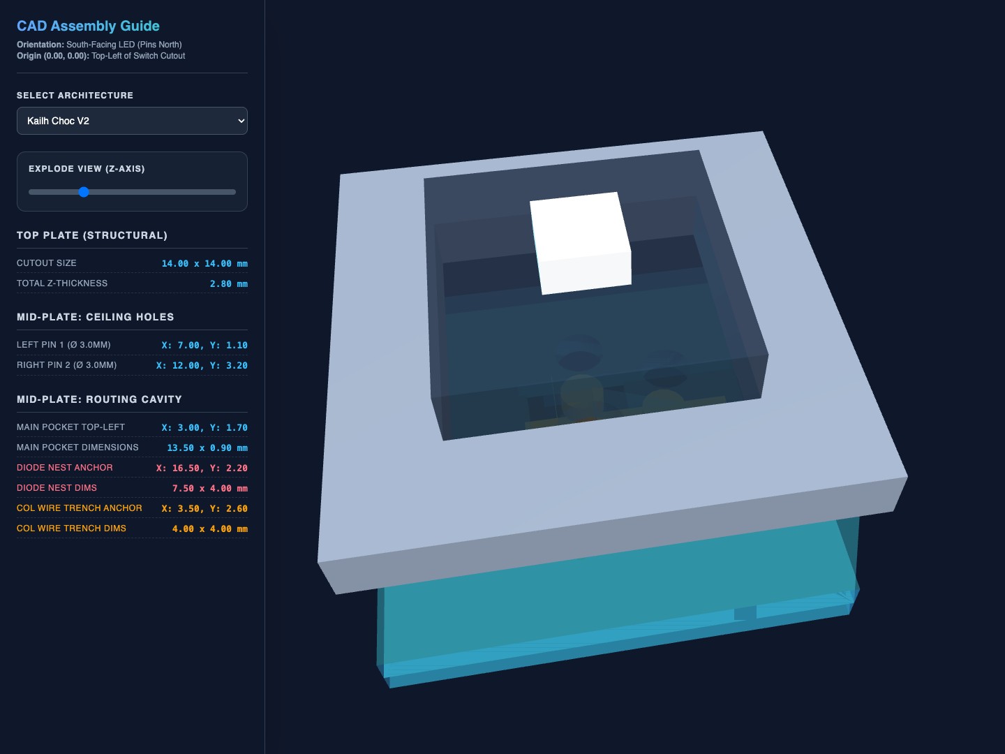 Initial single-switch proof of concept: A flush mid-plate holding the hotswap socket and diode captive below the top plate.
A printed mid-plate was mounted flush against the underside of the switch plate. Recessed pockets seated both the hotswap socket and diode body. This confirmed that switch pins could bottom out securely into socket leaves without floating in mid-air. Sockets and diodes remained firmly locked in plastic rather than relying on solder joints for mechanical support.
Parametric Switch Profiles
Hard-coding dimensions for a single switch model limits future maintenance and experimentation across different builds.
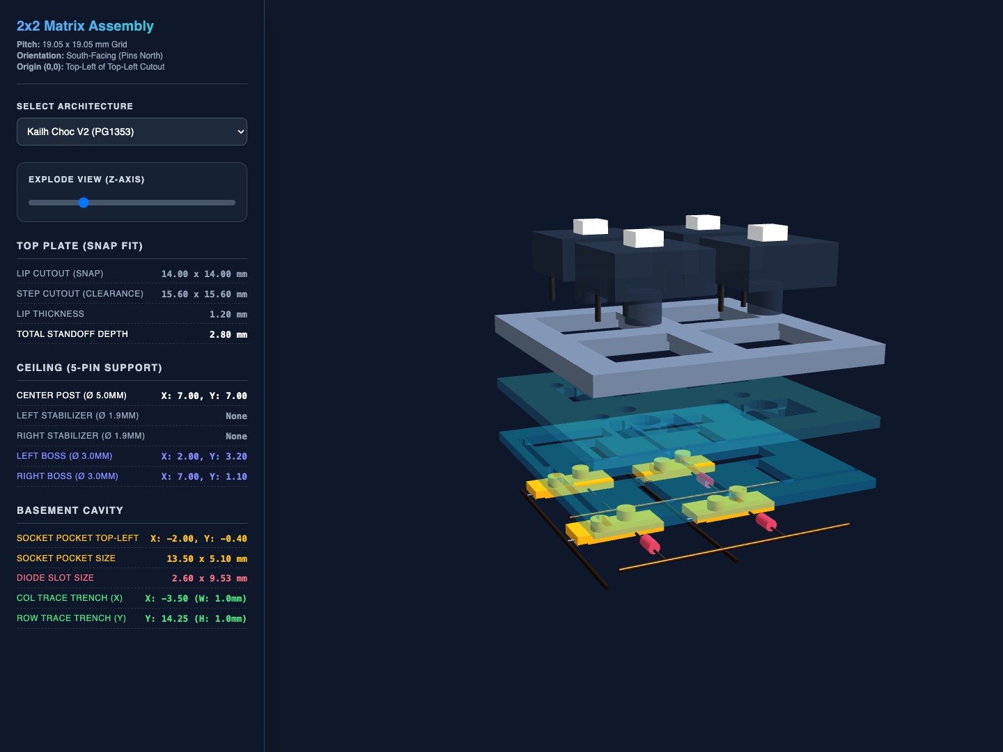 Parametric CAD assembly: Pocket coordinates and pin clearances adjust dynamically across switch footprints.
The CAD model was rebuilt parametrically to accommodate multiple switch standards: Kailh Choc V1, Choc V2, Gateron KS-33, and standard Cherry MX. Changing the primary switch parameter automatically recalculates socket offsets, center post diameters, and plate cutouts. This parametric baseline allows testing different switch formats without redrawing plate assemblies from scratch.
The 2x2 Matrix Grid
Validating a single switch pocket confirms local fitment, but it does not test array tiling or conductor paths.
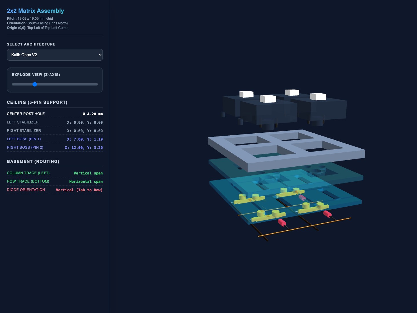 Tiling the geometry: A 2×2 grid establishing switch spacing and inter-switch wiring routes.
The geometry was tiled into a 2×2 grid at standard 19.05 mm spacing. Scaling the footprint introduced the physical challenge of routing conductors between adjacent switches. Inter-switch spacing highlighted the need for dedicated, continuous wire channels running along rows and columns to keep conductors organized and isolated.
The Tray-Loaded Grid
Stacking multiple loose intermediate plates introduced alignment play and assembly friction.
 Consolidating the structure: A top-loaded base tray integrating socket pockets and wire beds beneath a top plate.
The loose stack was consolidated into a rigid, top-loaded base tray with a solid floor. Socket pockets and diode recesses were carved directly into the tray substrate. The top switch plate and spacer drop straight over the loaded components, sandwiching them rigidly. This reduced part count and eliminated component shift during final fastening.
The Dual-Layer Skeleton
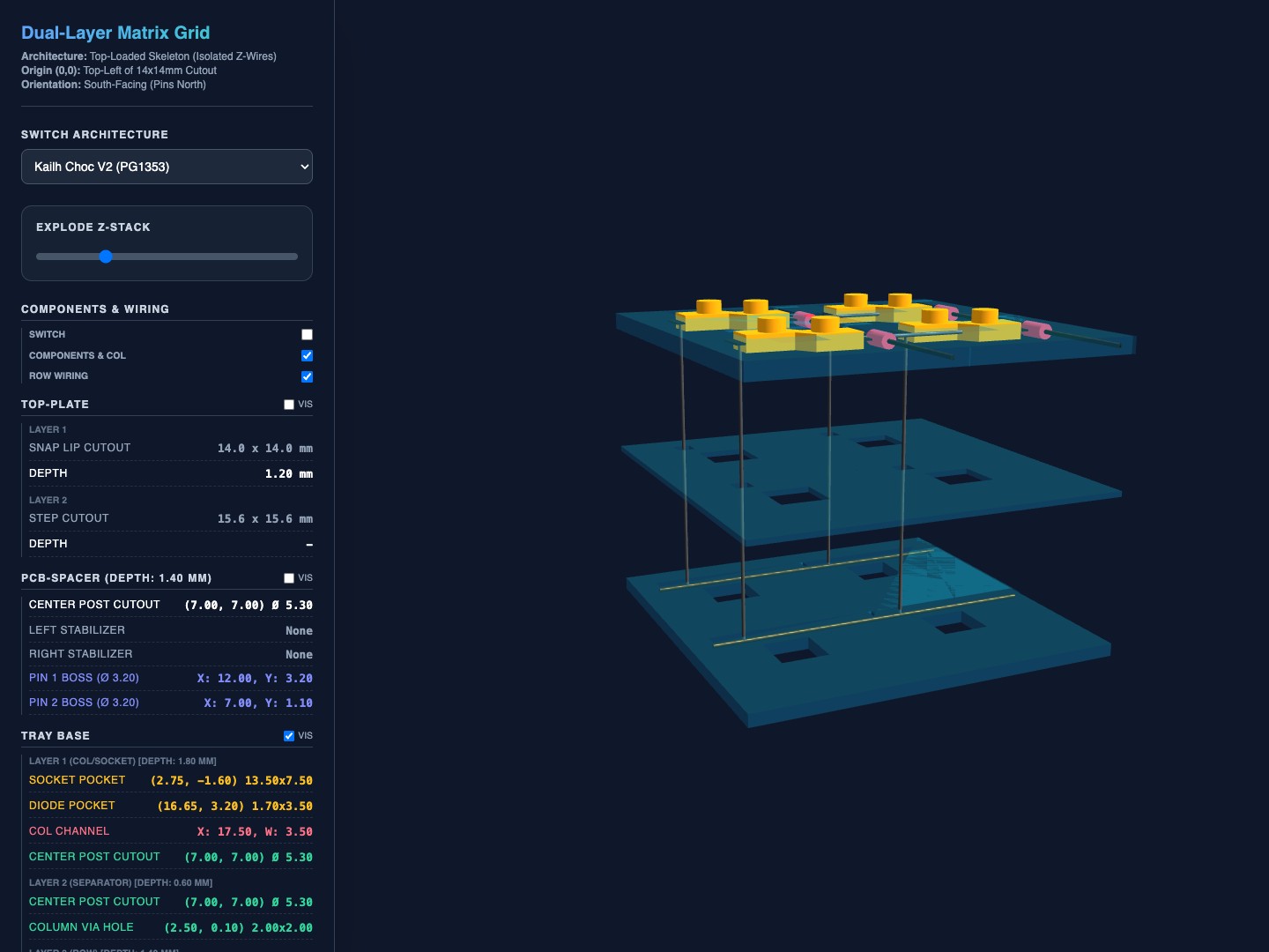
Running intersecting row and column conductors in a single physical plane creates an unacceptable risk of electrical shorts.
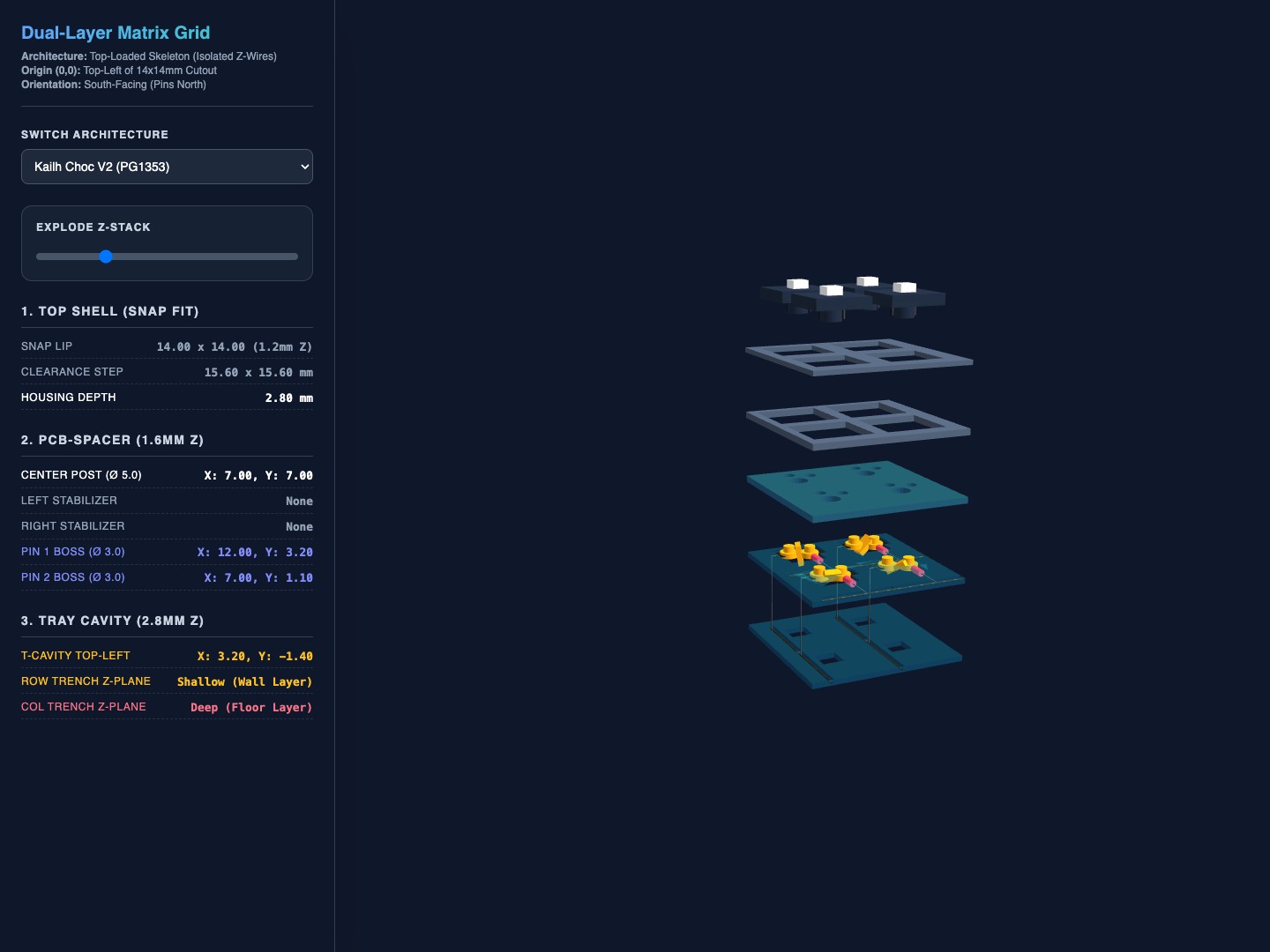
Isolated Z-wiring: Row channels and column channels separated into distinct vertical planes.
The tray architecture was split across three distinct Z-levels. Column channels run along the bottom level, while row channels run along the top level. A thin intermediate separator isolates the conductors, interrupted only by vertical via holes where specific electrical connections cross layers. Row and column wires remain physically segregated, eliminating accidental shorts and joint flex entirely.
Multi-Layer Plate Stackup
The finalized architecture establishes three core mechanical assemblies:
- Top Plate: Two-layer profile featuring a 14.0 mm snap lip that retains switch housings, backed by a 15.6 mm clearance step.
- PCB Spacer: A 1.4 mm intermediate layer that brings socket bosses flush against switch bases while clearing center posts.
- Tray Base: A three-tier substrate containing socket pockets, diode beds, lower column channels, isolation floor, and upper row channels.
Solid-core copper bus wires press directly into printed trenches and stay captive by friction. Assembly becomes systematic and repeatable, eliminating freehand wire bending.
With the plate stackup defined, the next task was evaluating switch options and physical tolerances in Step 2: Testing and Selecting Switches.